Topping D50 DAC Reverse engineering
Fine example of anger-driven development
Intro:
I was gifted this USB DAC as broken. The previous owner connected 12V adapter to it, instead of the 5V one. After I replaced damaged components, I run to problem with missing FW for STM8 MCU.
I tried to contact the manufacturer asking for the FW and my request was declined.
Even more given that the DAC is long obsolete

Damage done:
On the board there are 5 LDOs and 2 SMPS.
All LDOs are regulating to +3V3. They are used to generate:
- +3V3 for XU208 VCC
- +3V3 for I2S DAC Digital VCC
- +3V3 for left channel I2S DAC Analog VCC
- +3V3 for right channel I2S DAC Analog VCC
- +3V3 for STM8 MCU
SMPS:
- +1V0 for XU208m MCU core
- +/- 8V for analog output amplifiers and OLED
This OLED display is not equpped with integrated DC-DC converter, thats why it needs +3V3 and +8V.
The overvoltage event caused the XU208 core SMPS and the SMT8 LDO failure, damaging said ICs.
Also the OLED screen controller got damaged.
HW overview
Board picture:
(I didn't wanted to wait for the correct replacement part, so I replaced STM8 LDO with 1117 type regulator and the XMOS core SMPS with cheap DC-DC converter. The board is missing the XU208, that I left unpopulated during STM8 FW development)
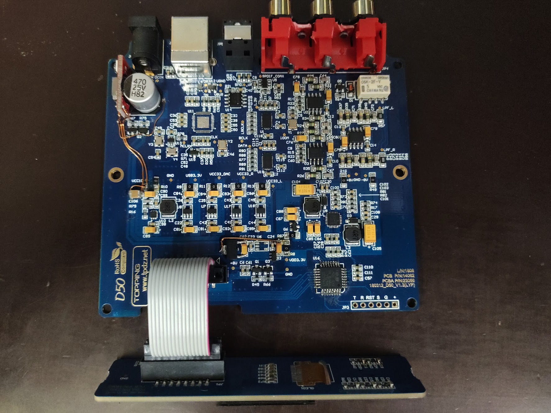
The D50 DAC is equpped with:
- two ES9038Q2M I2S DAC ICs, each for one audio channel
- XMOS XU208-128-QF48-C10 MCU, acting as USB to I2S bridge
- STM8S005K6T6C MCU, that controll OLED, LPF Relay, power to board, buttons and configures DAC ICs via I2C
- WEO064128A 64x128 SPI OLED
- One power button and 5-way switch
The ES9038Q2M is stereo DAC, but each is configured to output on both analog channels only L/R digital input in order to reduce noise.
I would expect that the outputs will be tied with som resistance, but they are connected dirrectly with copper trace.
The DACs are confirured over I2C by the STM8.
I2C Address:
- 0x90 for left audio channel
- 0x91 for right audio channel
The SPDIF input, both optical and coax is routed to both DAC ICs.
- Optical to GPIO1 (SPDIF input 4)
- Coax to GPIO2 (SPDIF Input 5)
Coaxial SPDIF input is routed via capacitor to dual SOT-23-6 inverter, with both gates in series to act as non-inverting signal conditioning buffer.
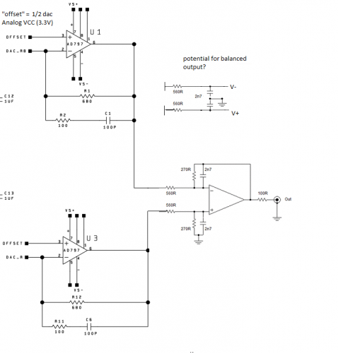
The output from DACs is routed to the OPA1612A op-amp. From what I found, it looks like the output stage is designed this way:
XMOS FW is stored on W25Q40CL SPI FLASH, luckily I was able to find this FW on archive.org.
Pinouts:
STM8S005K6T6C
| STM8 Pin | Board function | Note | STM8 Pin | Board function | Note |
|---|---|---|---|---|---|
| 1 | STM8 Reset | 17 | XU208 Pin 35 | ||
| 2 | DAC Reset | 18 | Sys PWR Btn | ||
| 3 | Output Relay ctrl | 19 | OLED PWR En | ||
| 4 | GND | 20 | OLED RST | ||
| 5 | VCAP | 21 | OLED CS | ||
| 6 | VCC | 22 | OLED D0(CLK) | ||
| 7 | VCCIO | 23 | OLED D1(MOSI) | ||
| 8 | 5-Way sw. right | HW Pull-up | 24 | OLED A0(DC) | |
| 9 | VCCA | 25 | BRD PWR En | ||
| 10 | GNDA | 26 | SWIM | ||
| 11 | I2C SDA | DAC Ctrl | 27 | XU208 Pin 11 | |
| 12 | I2C SCL | DAC Ctrl | 28 | XU208 Pin 13 | |
| 13 | 5-Way sw. down | HW Pull-up | 29 | XU208 Pin 36 | |
| 14 | 5-Way sw. up | HW Pull-up | 30 | UART TX (JP2) | UART2_TX |
| 15 | 5-Way sw. center | HW Pull-up | 31 | UART RX (JP2) + XU208 Pin 30 | UART2_RX |
| 16 | 5-Way sw. left | HW Pull-up | 32 | NC |
XU208-128-QF48-C10
| XU208 Pin | Board function | Note | XU208 Pin | Board function | Note |
|---|---|---|---|---|---|
| 1 | BCLK | 25 | VCC | ||
| 2 | LRCLK | 26 | NC | ||
| 3 | NC | 27 | X0D16 - MCLK Sel. | 0:45.158 MHz, 1:49.152 Mhz | |
| 4 | NC | 28 | NC | ||
| 5 | NC | 29 | NC | ||
| 6 | NC | 30 | X0D14 - STM8 Pin 31 | STM8 UART RX | |
| 7 | VCCIO | 31 | VCCIO | ||
| 8 | VCC | 32 | VCC | ||
| 9 | X0D1 - FLASH CS | 33 | MCLK | ||
| 10 | X0D10 - FLASH CLK | 34 | NC | ||
| 11 | X0D00 - STM8 Pin 27 | 35 | X0D27 - STM8 Pin 17 | ||
| 12 | X0D04 - FLASH DI | 36 | X0D28 - STM8 Pin 29 | ||
| 13 | X0D11 - STM8 Pin 28 | 37 | NC | ||
| 14 | X0D05 - FLASH DO | 38 | VCC | ||
| 15 | X0D06 - FLASH WP | 39 | PLL_AVCC | ||
| 16 | X0D07 - FLASH HOLD | 40 | OTP_VCC | ||
| 17 | USB_VCC +3V3 | 41 | RST (XU208) | ||
| 18 | USB_VBUS | 43 | CLK | XU208 CLK - 24MHz | |
| 19 | USB_RTUNE | 43 | NC (JTAG TMS) | ||
| 20 | USB_DP | 44 | NC (JTAG TCK) | ||
| 21 | USB_DM | 45 | NC (JTAG TDI) | ||
| 22 | USB_VCC | 46 | NC (JTAG TDO) | ||
| 23 | NC | 47 | NC | ||
| 24 | NC | 48 | I2S DAT |
Writing new SW:
As the STM8 for which I'm missing the firmware is responsible board power, OLED, button and DAC configuration, I needed to re-implement all of this.
To avoid Eclipse based IDE, I used STM8-SPL-SDCC project.